Our Research Tool (中文版網頁製作中):
|
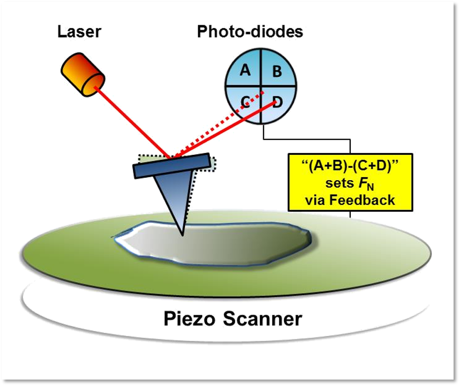
We use atomic force microscope (Bruker Multimode 8 AFM) to investigate the amazing properties of nanomaterials. As shown in the following figure, an AFM has has 4 basic components, including a cantilever with a sharp probe to scan the sample surface, a piezoelectric scanner to perform sample scanning, a laser shining on the back of the cantilever, and the the photo-diodes to collect the reflected laser light to track the motion of the cantilever. An electronic feedback loop is used to maintain a constanct setpoint (e.g. the normal force that the probe applies to the sample) between the probe and the sample surface during scanning such that the topography information of the sample can be obtained. |
 |
 |
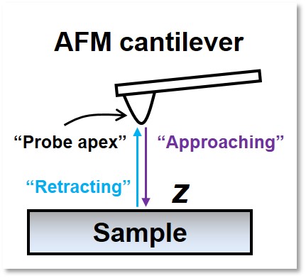
| *The
basic components of an AFM. |
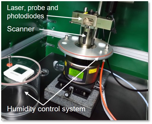
*Our
Bruker Multimode 8 AFM equipped with humidity control system in a home-built acroustic proof environment |
| The follwoing images obtained by scanning electron microscope shows a typical AFM probe. The green dashed circle mark the position of ths sharp tip. Because of the small tip apex(usuallly < 10 nm), a high resolution topography image of sample can be easily obtained with AFM. |
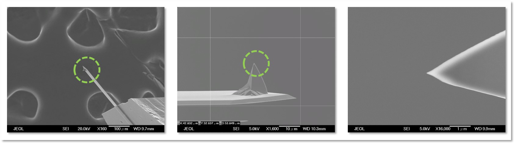 |
| *SEM images of a
typical AFM cantilever. The green dashed circle indicates the position
of the sharp probe, which is used to scan over the sample surface. The zoom-in image of the tip apex is shown on the right. |
| Based
on this fundemental principle, there are different AFM operation modes
for the investigation of various physical properties. The
following is
a summary of what our AFM system can do. |
| 1. Topography Imaging (both in liquid and ambient phases): Contact mode,
tapping mode and the novel peakforce tapping mode (Scansyst). |
 |
 |
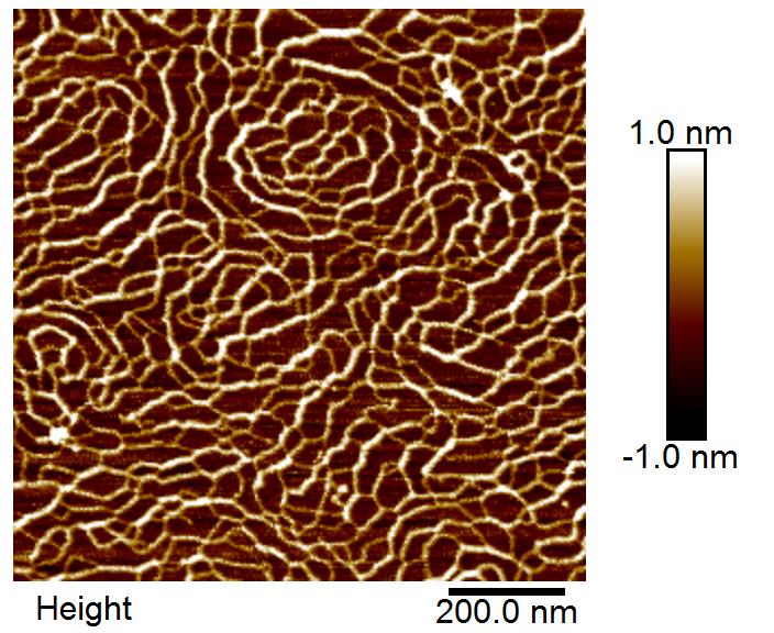
| *Tapping
mode: Double strand DNA on mica. |
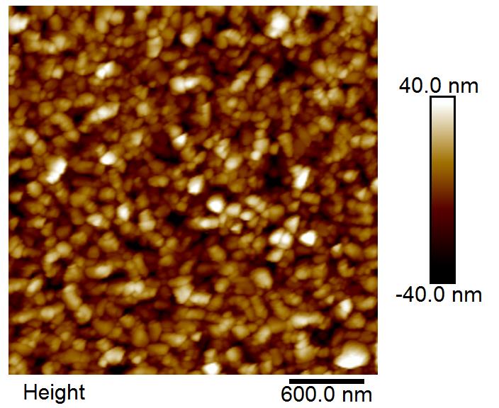
*Tapping
mode: Zinc Oxide thin film on sapphire. |
 |
 |
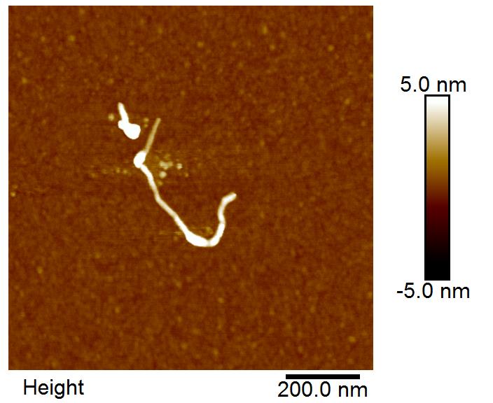
| *Scansyst:
CVD grown double walled carbon nanotube on silicon. |
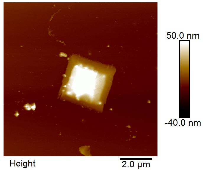
*Scansyst:
PbS nanosheet on silicon. |
 |
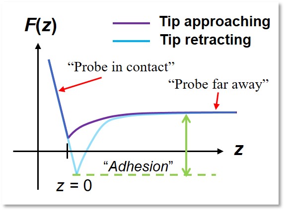 |
| *Schematic
showing a typical force-distance curve acquired by AFM. |
|
 |
|
| *The
force-distace curve provides information about the interaction between
the probe apex and the sample, which can be used to perform
nano-indentation experiments to study nanomechanical properties
of materials. It can also be used to perform single molecule force
spectroscopy to investigate the bio-mechanical properties of molecules
such as DNA. |
|
|
3.
Nano-mechanical Measurement: Peak Force quantitative
nanomechanical mapping
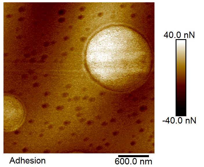
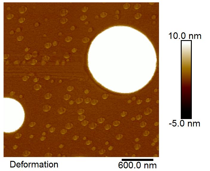
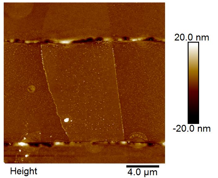
(PF QNM). We can simultaneously obtain the topography and elastic modulus mapping of a sample surface. The following is a series of images of PS-LDPE (ethylene-octene copolymer) obtained by using PF QNM. |
 |
 |
| *PF
QNM: Topography image of PS-LDPE. |
*PF QNM: Adhesion image of PS-LDPE. |
 |
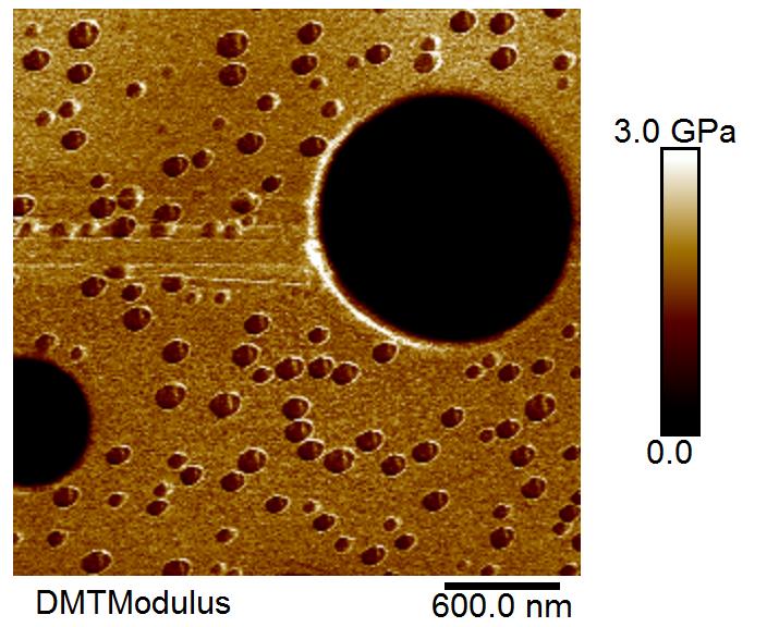 |
| *PF QNM: Deformation image of PS-LDPE. | *PF QNM: Elasticity image of PS-LDPE. |
4.
Electrical Measurement: Electrostatic Force Microscopy, Kelvin Probe
Force Microscopy, and
Conducting AFM.
 |
 |
| *Tapping
mode: Single layer raphene with gold electrodes (top and bottom). |
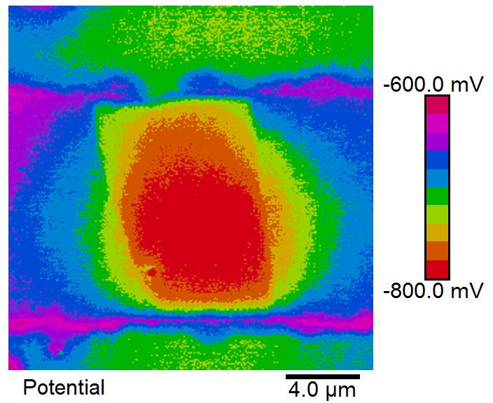
*KPFM:
Variation of surface potential across the graphene device. |
 |
|
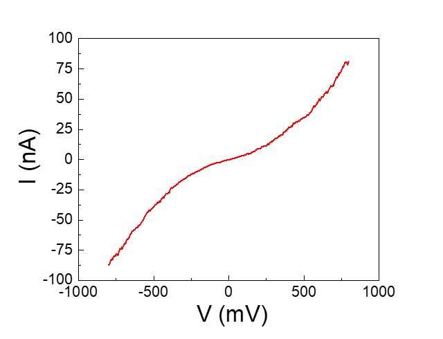
| *CAFM:
IV curve obtained from a conducting polyer thin film. |
| 5.
Combined mechanical and electrical measurements: Peakforce
Tunneling AFM (PF TUNA), permitting "simultaneous" measurements of surface topography, elastic moduli, adhesion, deformation and electrical properties of a sample. |
6.
Magnetic Measurements: Magnetic Force Microscopy.
 |
 |
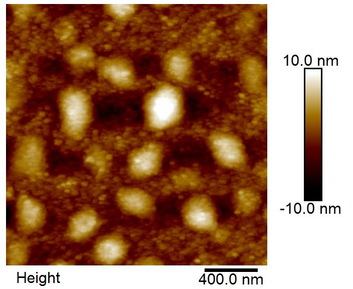
| *Tapping
mode: Topography image of a Co50Pd50 alloy thin film. |
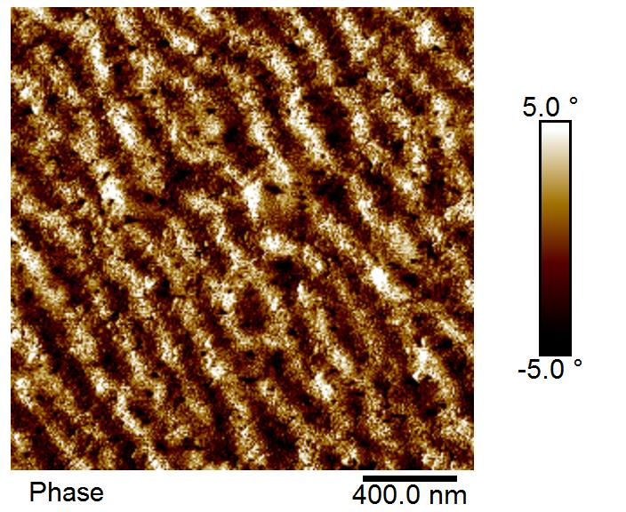
*MFM:
Variation of magnetic domains across the Co50Pd50 alloy thin film surface. |
Other Facilities and Instruments:
| Milli-Q ultra pure water system, Harrick Plasma cleaner (oxygen and argon), Olympus optical microscope, Stereo microscope, chemical fume hoods, oven system with mechanical pump and cold trap, UV lamps etc. |
Research
Projects:
1.
Nanoscopic friction of 2D-material coated surface and oxide
nanomaterials:
| Friction is one of the oldest problems in physics, but a comprehensive understanding about its origin from the atomic or molecular level, or the capability to control it in various environments is far from being complete. Through AFM friction measurements, we aim to understand the fundemental mechanism of friction at the nanoscale. |
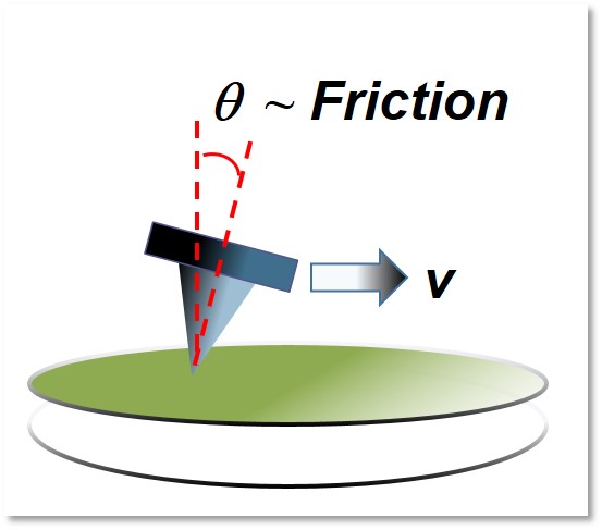 |
| *During the
friction measurement, the normal force can be controlled by the normal
deflection of AFM cantilever, while the friction is measured through
the torsional motion of the cantilever. |
|
One of
our current interest is the frictional properties of 2D nanomaterials, which can be used as protection or lubrication layers for NEMS. Understanding
their frictional
properties will be important for developement of NEMS
devices
2. Nano-mechanical, frictional and electrical properties of conducting polymer thin films: Conducting polymers have
promising applications in modern electronics such as the screen display for
smart phones. They also have potential applications such as protective
coatings, artificial muscles, actuators, photovoltaics
and flexible
electronics, which could be integrated in future NEMS for multifunctional applications.
Through
the manipulation of polymer structure, we aim to understand the correlation between its
mechanical and
electrical properties at the nanoscale which may benifit future NEMS design.
3. Tribo-electric effect of polymers at the nanoscale.
Tribo-electric effect is an
important physcial phenomena that we have all experienced in our
daily life. Through the nanoscale frictional and
electrical AFM
measurements, we aim to gain more clear insight into its
fundemental mechanism. We hope our findings can improve the efficiency of novel triboelectric nanogenerators (TENG).
|